
Staying ahead in hardware innovation means understanding not just the devices we use, but the technologies shaping what comes next. If you’re searching for clear, reliable insights into emerging interface technologies, next-generation device concepts, and the materials powering tomorrow’s breakthroughs, you’re in the right place.
This article explores how advanced electronic materials are transforming device performance, enabling smarter interfaces, improved energy efficiency, and entirely new hardware possibilities. From flexible substrates to high-performance semiconductors and novel sensor integrations, we break down what’s changing and why it matters.
Our analysis draws on current engineering research, prototype developments, and real-world implementation trends across the tech ecosystem. The goal is simple: give you a focused, technically grounded overview that helps you understand where innovation is happening now—and how it will shape the next wave of devices. Whether you’re an engineer, investor, or tech enthusiast, you’ll gain practical insight into the technologies driving the future of hardware.
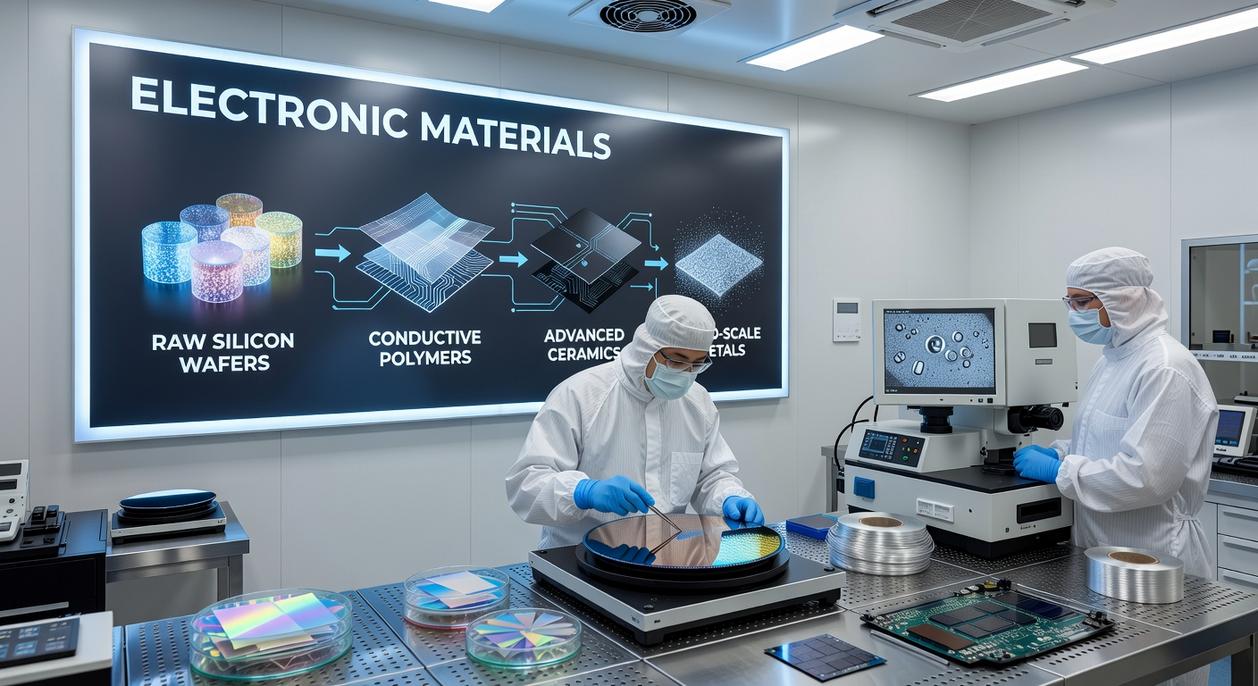
Last year, I held a prototype chip that overheated in my palm—an unsettling reminder that silicon is nearing its limits. Since then, labs have pivoted toward advanced electronic materials to keep progress alive. So what’s stepping in?
- Gallium nitride (GaN): handles higher voltages and powers chargers on store shelves.
- Silicon carbide (SiC): boosts efficiency in electric vehicles, extending driving range.
- Two-dimensional materials like graphene: promise flexible sensors.
Meanwhile, skeptics argue silicon still has room to scale. However, quantum tunneling and heat density say otherwise. Consequently, tomorrow’s foldable, wearable, and AI-driven devices will rely on this material toolkit.
Graphene and 2D Materials: From Lab Theory to Thermal Reality
Graphene—a single atomic layer of carbon arranged in a hexagonal lattice—was once the poster child of materials science hype. Touted as 200 times stronger than steel and exceptionally conductive (Novoselov et al., Science, 2004), it sounded like science fiction. But hype doesn’t cool a processor. Thermal reality does.
Let’s compare Graphene vs. Copper Heat Spreaders:
- Thermal Conductivity: Graphene can exceed 2,000 W/mK in ideal conditions, while copper averages around 400 W/mK (Balandin, Nature Materials, 2011).
- Weight & Thickness: Graphene films are ultra-thin and lightweight; copper adds bulk.
- Flexibility: Graphene bends; copper resists (and sometimes cracks under repeated stress).
Some skeptics argue copper is cheaper, easier to source, and “good enough.” Fair point. Copper has decades of manufacturing infrastructure behind it. But in compact smartphones and performance laptops, “good enough” often means thermal throttling—when processors reduce clock speeds to prevent overheating. Graphene-based heat spreaders dissipate heat faster, enabling sustained performance under load (yes, that means smoother gaming and fewer laptop fan meltdowns).
Beyond thermal management, chemical vapor deposition (CVD)—a process that grows thin films atom-by-atom—has shifted graphene from lab curiosity to scalable component. Compared side-by-side:
- Traditional Materials: Rigid, limited sensitivity, bulk fabrication.
- Graphene & 2D Materials: Flexible displays, ultra-sensitive sensors, integration into advanced electronic materials stacks.
Critics still question cost curves and defect control. They’re right to. Scaling perfection is hard (ask any chipmaker). Yet as production improves, graphene is transitioning from “wonder material” to engineered solution—less Marvel origin story, more manufacturing milestone. The question isn’t whether it works. It’s where it delivers the clearest advantage.
Gallium Nitride (GaN): The New Standard for Power Efficiency
For decades, silicon has been the backbone of power electronics. But it has a flaw: inefficiency. During power conversion—the process of changing electrical energy from one form to another—silicon devices lose energy as heat. According to the U.S. Department of Energy, power conversion losses can account for 5–10% of total electricity use in the United States alone. That wasted energy translates into bulkier cooling systems, larger components, and higher operating costs.
Gallium Nitride (GaN), a wide-bandgap semiconductor (meaning it can handle higher voltages and temperatures than traditional silicon), changes that equation. Research published in IEEE journals shows GaN transistors can switch up to 10x faster than silicon MOSFETs while reducing energy losses by as much as 40% in certain applications.
The clearest proof is in consumer chargers:
- 65W GaN adapters are often 40% smaller than silicon equivalents.
- Higher switching frequencies allow smaller transformers and capacitors.
- Reduced heat output improves lifespan and safety.
(If you’ve ever touched a laptop charger that felt like a mini space heater, you understand the upgrade.)
At scale, the impact is even more measurable. Data centers—responsible for roughly 1–1.5% of global electricity use (IEA, 2023)—benefit from GaN’s higher efficiency and reduced cooling loads. In EV powertrains, improved power density means lighter systems and extended range. LiDAR platforms also leverage GaN’s high-frequency performance for sharper signal precision.
As demand grows for advanced electronic materials, GaN is proving not just viable—but essential. Even adjacent fields like swarm robotics and distributed intelligence systems rely on compact, efficient power architectures to scale effectively.
Perovskites: The Dual-Threat in Solar and Display Technology
Perovskites are a class of materials defined by their distinctive crystal structure—a specific atomic arrangement that acts like a perfectly organized apartment complex for electrons. Because of this structure, they excel at absorbing and emitting light. In other words, they’re the overachievers of advanced electronic materials.
In solar technology, perovskite cells function like ultra-thin solar sponges. Traditional silicon panels are reliable but bulky—think brick houses. Perovskites, by contrast, are more like high-tech tents: lightweight, flexible, and potentially transparent. Not only have lab efficiencies surpassed 25% (National Renewable Energy Laboratory), but manufacturing could also be cheaper due to lower processing temperatures. That’s a big deal.
Meanwhile, in displays, perovskite quantum dots (nanometer-sized light emitters) operate like precision paintbrushes, producing intensely pure colors. As a result, they may outperform current QLED technology in brightness and energy efficiency. Imagine upgrading from HD to 4K for your eyeballs (yes, it’s that noticeable).
Of course, skeptics point to stability issues—heat and moisture have historically degraded performance. However, recent encapsulation breakthroughs are acting like protective raincoats, significantly extending lifespan. Consequently, commercialization no longer feels theoretical. Instead, it feels imminent.
The Next Wave: Carbon Nanotubes and Quantum Dots
Carbon Nanotubes (CNTs)—rolled graphene sheets—promise to replace copper interconnects, easing nanoscale data bottlenecks. I once dismissed them as lab hype; that was a mistake. Chipmakers hit resistance limits faster than expected, and CNT prototypes proved shockingly resilient. Quantum Dots (QDs), nanocrystals behind QLED brilliance, seemed “just display tech” (turns out, never say just). Now they’re advancing medical imaging and quantum computing with precise photon control. The lesson? Betting against advanced electronic materials because commercialization looks distant can blind you to compounding breakthroughs. Today’s fringe experiment often becomes tomorrow’s hardware backbone. Stay curious.
The new blueprint for hardware engineering is being rewritten by materials, not just microchips. For decades, silicon ruled; now GaN, graphene, and perovskites challenge its limits. These advanced electronic materials promise faster switching, cooler operation, and brighter, thinner displays. Skeptics argue silicon still dominates supply chains, and they’re right to question scalability. I don’t pretend every lab breakthrough survives manufacturing. Yet three shifts feel undeniable: 1. Power electronics moving to GaN. 2. Flexible interfaces enabled by graphene. 3. Next-gen displays driven by perovskites. The timeline is uncertain, but momentum is real, reshaping what devices can become. Much remains genuinely unknown.
The Future Is Built on Smarter Materials
You came here to understand how advanced electronic materials are reshaping device performance, interface design, and next-generation hardware. Now you’ve seen how breakthroughs in conductivity, flexibility, thermal management, and miniaturization are pushing innovation beyond traditional limits.
The real challenge isn’t knowing these materials exist — it’s keeping up with how fast they’re evolving and figuring out which advancements actually matter for your designs, prototypes, or product roadmap. Falling behind means slower development cycles, higher costs, and missed competitive opportunities.
The smartest move you can make now is to stay ahead of material innovation and apply these insights strategically to your next build. Track emerging research, evaluate integration pathways early, and align your hardware decisions with the materials that will define tomorrow’s performance standards.
If you’re serious about staying competitive, start leveraging trusted, industry-leading insights used by thousands of forward-thinking engineers and innovators. Explore the latest updates, apply what fits your roadmap, and take action today — because the next breakthrough won’t wait.
 Hazel Brinkleyanday has opinions about advanced concepts. Informed ones, backed by real experience — but opinions nonetheless, and they doesn't try to disguise them as neutral observation. They thinks a lot of what gets written about Advanced Concepts, Tech Innovation Updates, FNTK Hardware Engineering Insights is either too cautious to be useful or too confident to be credible, and they's work tends to sit deliberately in the space between those two failure modes.
Reading Hazel's pieces, you get the sense of someone who has thought about this stuff seriously and arrived at actual conclusions — not just collected a range of perspectives and declined to pick one. That can be uncomfortable when they lands on something you disagree with. It's also why the writing is worth engaging with. Hazel isn't interested in telling people what they want to hear. They is interested in telling them what they actually thinks, with enough reasoning behind it that you can push back if you want to. That kind of intellectual honesty is rarer than it should be.
What Hazel is best at is the moment when a familiar topic reveals something unexpected — when the conventional wisdom turns out to be slightly off, or when a small shift in framing changes everything. They finds those moments consistently, which is why they's work tends to generate real discussion rather than just passive agreement.
Hazel Brinkleyanday has opinions about advanced concepts. Informed ones, backed by real experience — but opinions nonetheless, and they doesn't try to disguise them as neutral observation. They thinks a lot of what gets written about Advanced Concepts, Tech Innovation Updates, FNTK Hardware Engineering Insights is either too cautious to be useful or too confident to be credible, and they's work tends to sit deliberately in the space between those two failure modes.
Reading Hazel's pieces, you get the sense of someone who has thought about this stuff seriously and arrived at actual conclusions — not just collected a range of perspectives and declined to pick one. That can be uncomfortable when they lands on something you disagree with. It's also why the writing is worth engaging with. Hazel isn't interested in telling people what they want to hear. They is interested in telling them what they actually thinks, with enough reasoning behind it that you can push back if you want to. That kind of intellectual honesty is rarer than it should be.
What Hazel is best at is the moment when a familiar topic reveals something unexpected — when the conventional wisdom turns out to be slightly off, or when a small shift in framing changes everything. They finds those moments consistently, which is why they's work tends to generate real discussion rather than just passive agreement.