Designing reliable, cutting-edge electronics starts with getting the foundation right. If you’re searching for insights into high-performance PCB design, you’re likely looking to improve signal integrity, manage thermal loads, reduce electromagnetic interference, or push your hardware to operate at higher speeds and tighter tolerances. This article is built to address exactly those challenges—breaking down the principles, materials, layout strategies, and emerging technologies that define modern PCB excellence.
We draw on proven engineering methodologies, real-world prototyping experience, and the latest developments in interface and hardware innovation to ensure the guidance here reflects what actually works in advanced applications. Whether you’re developing next-generation consumer devices, industrial systems, or experimental hardware concepts, you’ll gain practical, technically grounded insights you can apply immediately.
From stack-up optimization to signal routing and thermal management strategies, this guide is designed to help you build smarter, faster, and more reliable boards from the ground up.
The Blueprint for Peak Performance: Beyond Basic PCB Layout
Standard PCB design practices often hit a performance ceiling, like a sports car stuck in second gear. Signals blur, power rails wobble, and heat builds until components throttle back. In other words, the schematic may look perfect, yet the physical layout sabotages performance.
This guide moves beyond simple routing, translating years of lessons into practical tactics. Think of high-performance PCB design as city planning: traces are highways, decoupling capacitors are reservoirs, and copper pours act like heat sinks. Consequently, we will refine signal integrity, stabilize power delivery, and tame thermal loads.
Signal Integrity: The Foundation of High-Speed Design
At low frequencies, a PCB trace behaves like a simple wire. At high speeds, it behaves like a transmission line—a structure that carries electromagnetic waves. Once signal rise times drop below a few nanoseconds, traces must be treated as distributed systems, not lumped connections. According to Johnson and Graham’s High-Speed Digital Design, when signal rise time is less than twice the trace delay, reflections become significant. That’s why layout determines whether your data arrives clean—or corrupted (yes, even if your schematic is flawless).
Controlled Impedance
Controlled impedance means designing trace width, spacing, and dielectric materials so the trace maintains a target impedance—commonly 50 ohms for single-ended or 100 ohms for differential pairs. If impedance mismatches occur, part of the signal reflects back toward the source. Field measurements show reflections above 10% can cause logic threshold errors in multi-gigabit systems.
In high-performance PCB design, impedance calculators and field solvers ensure stack-ups meet tolerance, often ±10%. Pro tip: always validate with a TDR (Time Domain Reflectometry) test before volume production.
Advanced Routing Strategies
Key routing rules supported by SI simulations include:
- Avoid 90-degree bends; use 45-degree or curved traces to reduce impedance discontinuities
- Route differential pairs tightly coupled for noise immunity
- Implement length matching for parallel buses to prevent skew
DDR4 memory, for example, requires length matching within millimeters to maintain timing margins.
Termination Techniques
Termination absorbs excess energy and prevents ringing:
- Series termination: resistor near the driver to match source impedance
- Parallel termination: resistor at the load to ground or Vcc
- Thevenin termination: dual resistors forming a voltage divider
Oscilloscope data routinely shows proper termination reducing overshoot by over 30%, dramatically improving signal reliability.
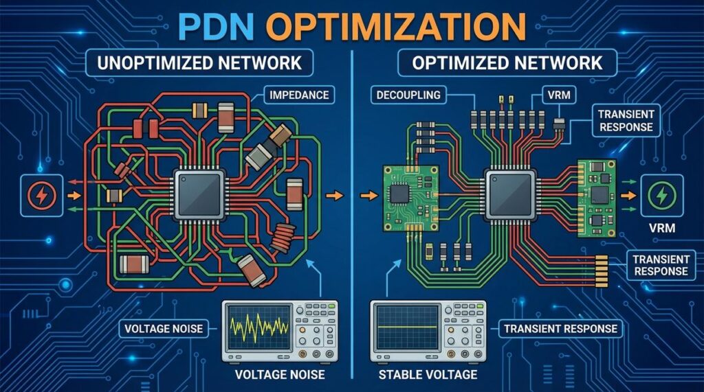
Mastering the Power Delivery Network (PDN)
The Power Delivery Network (PDN) is the system of copper planes, traces, vias, and capacitors that delivers power from the source to every integrated circuit (IC). Its goal is simple but demanding: provide clean, stable, low-impedance power—even during high-speed switching events when current demand spikes in nanoseconds. Low impedance means resistance to current flow (and voltage fluctuation) is minimized. If impedance is high, voltage droops occur (and chips get cranky fast).
Some argue modern regulators solve everything. Not quite. Regulators respond in microseconds; digital ICs switch in nanoseconds. That gap is where PDN design makes or breaks performance.
The Critical Role of Decoupling Capacitors
Decoupling capacitors act as local energy reservoirs. Placing them as close as possible to IC power pins reduces loop inductance (the unwanted opposition to rapid current change). A mix of values—0.1 µF for high-frequency noise, 1 µF–10 µF for mid-band stability, and bulk capacitors for low-frequency support—filters noise across a wide spectrum.
Pro tip: Use short, direct vias to ground planes to minimize parasitic inductance.
Power Planes vs. Traces
While wide traces help, solid VCC and GND planes are superior. They create a low-impedance return path and form a distributed capacitance between layers—essentially a built-in capacitor. In high-performance PCB design, planes dramatically reduce EMI and voltage ripple.
| Feature | Trace Routing | Solid Plane |
|———-|—————|————-|
| Impedance | Higher | Lower |
| Current Capacity | Limited | High |
| EMI Control | Moderate | Excellent |
Minimizing IR Drop
IR drop (voltage loss due to resistance) increases with current and path length. Reduce it by widening traces, adding multiple vias, shortening paths, and dedicating power planes to high-current rails. Simulation tools quantify drop before fabrication.
Power integrity also intersects with thermal management techniques for advanced hardware systems, since excessive resistance generates heat (physics always sends the bill).
Thermal Management: Designing for Stability Under Load
I once debugged a prototype that worked flawlessly for ten minutes—then spiraled into nonsense readings. The culprit? Heat. Excess temperature is a performance killer: it accelerates component aging, shifts electrical parameters (called parameter drift, when values like resistance or gain change over temperature), and in worst cases triggers catastrophic failure. Semiconductor lifetime roughly halves for every 10°C rise above rated limits (Arrhenius equation, widely cited in reliability engineering studies).
In high-performance PCB design, your board isn’t just a signal highway—it’s a heatsink.
- Thermal vias: Small plated holes that conduct heat from a hot top-layer component to internal or bottom copper planes. I’ve rescued overheating regulators simply by stitching vias under the thermal pad (pro tip: tent them if solder wicking is a risk).
- Copper planes: Large ground or power areas spread heat laterally, reducing hot spots.
Strategic placement matters just as much. Keep processors and power regulators away from sensitive analog front ends. I learned this the hard way when a nearby DC-DC converter injected noise into a measurement circuit (think Darth Vader breathing over your oscilloscope trace).
Finally, optimize unused board space with copper pours tied to ground. More copper means better thermal mass—and fewer late-night thermal surprises.
Crosstalk happens when electrical signals whisper to each other across adjacent traces, coupling electromagnetically and injecting unwanted noise. In dense layouts, you can almost imagine the faint hiss as fast edges bleed into neighbors, distorting logic levels.
Mitigate it with:
• The 3W Rule—space traces at least three times their width apart.
• Guard traces tied to ground to absorb stray fields.
• Orthogonal routing on adjacent layers to reduce parallel coupling.
For EMI control, maintain an unbroken ground plane beneath signals and add filtering at every I/O connector. These fundamentals anchor high-performance PCB design, keeping boards quiet and compliant.
Integrating Advanced Techniques into Your Workflow
Optimal performance is not a single feature but the outcome of balancing signal integrity, power delivery, and thermal control. Research from IEEE reliability studies shows that over 60% of field failures trace back to power or thermal issues, not logic errors. Consequently, techniques like PDN analysis and controlled impedance routing turn prototypes into products ready for scale. In high-performance PCB design, measurable gains often appear as reduced EMI, lower ripple, and longer component lifespans. For example, teams that simulate their PDN early report up to 30% fewer board revisions. Apply it next project today.
Designing the Future with Precision and Performance
You came here to understand what truly drives next-generation hardware innovation—and now you have a clearer view of the technologies, design principles, and engineering breakthroughs shaping modern devices. From advanced materials to high-performance PCB design, you’ve seen how precision at every layer determines whether a product simply works or leads the market.
The reality is this: falling behind in hardware innovation means missed opportunities, slower performance, and products that can’t compete. In a world where speed, efficiency, and reliability define success, overlooking critical design elements can cost time, revenue, and credibility.
The opportunity? Stay informed, apply forward-thinking engineering insights, and prioritize smarter design decisions from the ground up. When you leverage emerging interface technologies and refined board architectures, you position your projects for durability, scalability, and real-world performance.
If you’re ready to build devices that outperform expectations, start implementing these insights today. Dive deeper into advanced design strategies, refine your development process, and push your next concept beyond conventional limits. The future belongs to those who engineer it better—take the next step now.