As artificial intelligence systems push the limits of traditional computing, interest in neuromorphic chip architecture is accelerating. Engineers, researchers, and tech enthusiasts alike are searching for clearer explanations of how these brain-inspired designs work, why they matter, and what they could mean for the future of devices and intelligent systems.
This article is built to answer that need directly. We break down the core principles behind neuromorphic design, explore how it differs from conventional processor architectures, and examine the real-world applications driving its development—from edge AI devices to next-generation robotics.
Our insights draw on current hardware research, emerging interface experiments, and ongoing advancements in chip fabrication techniques. By grounding the discussion in verified engineering concepts and active development trends, we aim to provide a reliable, technically sound overview that helps you understand not just the theory—but the practical impact—of this rapidly evolving computing paradigm.
Conventional processors separate memory and compute, forcing data to shuttle back and forth—a constraint known as the Von Neumann bottleneck. As a result, energy drains and latency climbs, especially in AI workloads. Neuromorphic chip architecture flips this script by co-locating memory and processing in neuron-like circuits. In theory, that enables massive parallelism and real-time learning. However, fabrication challenges, device variability, and programming models remain unsettled. Researchers debate whether analog components can scale reliably (physics rarely offers freebies). Still, early prototypes show orders-of-magnitude efficiency gains, suggesting brain-inspired hardware could redefine practical computing limits. Yet commercial viability remains uncertain today for now.
The Von Neumann Bottleneck: Why Traditional Chips Are Hitting a Wall
As neuromorphic chips usher in a new era of device architecture, understanding the software challenges they present, such as those outlined in our article on Python Error Oxzep7 Software, becomes essential for developers looking to harness their full potential.
To understand the Von Neumann bottleneck, we need a simple definition. Traditional computers separate the CPU (the processor that performs calculations) from RAM (the memory that stores data). That physical split means every instruction requires data to travel back and forth—like commuting across a crowded bridge every single time you need a file.
– Bottleneck
-
This constant movement creates a data traffic jam. In fact, memory access can consume more energy than computation itself (U.S. Department of Energy reports show data movement dominates power use in modern systems). Some argue faster buses and bigger caches solve this. They help—but they don’t remove the bridge. The distance still exists.
AI makes things worse. Machine learning models contain millions or billions of parameters—adjustable values that define how the model behaves. Training them means shuttling enormous datasets between CPU and memory nonstop. That’s why data centers consume terawatt-hours of electricity annually (IEA, 2023). It’s less “The Matrix” and more “rush hour on the 405.”
For decades, Moore’s Law—shrinking transistors to boost performance—masked this inefficiency. But as components approach atomic scales, gains slow (Nature, 2021). Critics say optimization is enough. Yet many engineers believe only new designs, like neuromorphic chip architecture, can truly break the wall.
Decoding the Brain’s Blueprint for Efficiency
To understand why engineers obsess over the brain, start with its core design principle: processing-in-memory. In simple terms, memory (synapses—the connections between neurons) and processing (neurons—the cells that transmit signals) live in the same place. There’s no constant back-and-forth data shuffle like in traditional computers. By contrast, most CPUs separate memory and processing, creating what’s called the von Neumann bottleneck—a traffic jam of data moving between two physically distinct areas (think commuters stuck on a single highway).
Equally important is parallelism at scale. The human brain contains roughly 86 billion neurons, many of which can operate simultaneously (Azevedo et al., 2009). Instead of handling one instruction at a time like a typical sequential processor, the brain runs countless operations in parallel. Imagine millions of light switches flipping independently rather than waiting their turn.
Then there’s event-driven processing, also known as sparsity. Neurons “spike” only when incoming signals cross a threshold. No meaningful signal? No spike. No energy burned. Meanwhile, in a standard chip clock cycle, billions of transistors toggle on and off whether meaningful work is happening or not (a bit like revving a car engine at every red light).
Key efficiency principles engineers study:
- Co-located memory and compute
- Massive parallel activity
- Energy use only when triggered
- Adaptive connection strength
Finally, learning and plasticity—or neuroplasticity—means synapses strengthen or weaken based on activity. “Cells that fire together, wire together” (Hebb, 1949). This adaptability is precisely what designers aim to emulate in neuromorphic chip architecture, bringing hardware closer to biological intelligence.
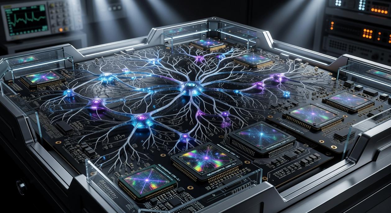
Engineering the Synapse: Key Components of Neuromorphic Chips
The first time I saw a neuromorphic demo on a lab bench, it didn’t look impressive. No flashy GPU rack. No roaring fans. Just a quiet board recognizing patterns in real time (almost suspiciously calm). That’s when it clicked: this wasn’t traditional computing—it was something closer to biology.
1. Artificial Neurons and Synapses
Engineers design silicon circuits that model neurons (cells that process signals) and synapses (connections that adjust signal strength). These can be digital (binary-based) or analog (continuous signal-based). Much like how your brain strengthens connections when learning a new skill, these circuits adjust weights to “learn” patterns. IBM’s TrueNorth and Intel’s Loihi chips demonstrate this principle in hardware (Merolla et al., 2014; Davies et al., 2018).
Some critics argue software simulations on GPUs are enough. Fair point—GPUs are powerful. But they consume significantly more energy for brain-like workloads (Sze et al., 2017). Hardware-level replication changes the efficiency equation.
2. The Role of Memristors
A memristor (memory + resistor) remembers how much charge has passed through it. That property makes it ideal for artificial synapses. When power is removed, it retains state—just like biological memory. HP Labs first demonstrated practical memristors in 2008 (Strukov et al., 2008).
3. Spiking Neural Networks (SNNs)
Instead of constant signals, SNNs communicate via discrete “spikes.” This event-driven model mirrors how real neurons fire only when necessary (think Morse code, but smarter).
4. Asynchronous Design
Traditional CPUs rely on rigid clock cycles. Neuromorphic systems often operate asynchronously—no central clock, just activity when events occur. That’s central to neuromorphic chip architecture and its low-power edge.
For a broader look at emerging hardware shifts, explore revolutionary device concepts that could redefine smart living.
Real-World Impact and Future Hurdles
Current Applications are moving from lab demos to deployment. Ultra-low-power sensors for IoT stretch battery life from months to years. Real-time pattern recognition in autonomous vehicles processes edge data without cloud lag (think reflexes, not round-trips). Advanced medical diagnostic tools flag anomalies in imaging faster than traditional chips.
A vs B: Classical CPUs execute sequential code; neuromorphic chip architecture mimics neural spikes for parallel inference.
The counterargument? Hardware breakthroughs should be enough. Not quite. The real bottleneck is software—new programming models and algorithms must match this radically different design. Toolchains remain immature and fragmented. Today.
The limits of today’s chips are measurable. Modern AI models can consume megawatt-hours of electricity during training, and data centers already account for about 1–2% of global power use (IEA). Meanwhile, the human brain runs on 20 watts. Clearly, brute-force scaling is unsustainable.
Neuromorphic chip architecture changes that equation. By merging memory and processing, it removes the “von Neumann bottleneck”—the latency caused by shuttling data back and forth. In turn, event-driven computation activates circuits only when signals fire, much like neurons.
IBM’s TrueNorth demonstrated millions of spiking neurons at milliwatt power levels. Think Jarvis in a helmet—highly efficient and parallel.
The Future of Neuromorphic Innovation Starts Now
You came here to understand how neuromorphic chip architecture is reshaping the future of computing—and now you have a clear picture of why it matters. From energy efficiency to real-time adaptive learning, this technology isn’t just an upgrade. It’s a fundamental shift in how machines process information.
The challenge has always been the same: traditional architectures can’t keep up with the growing demand for speed, efficiency, and intelligence at the edge. That bottleneck slows innovation, increases power consumption, and limits what next-generation devices can truly achieve.
Neuromorphic systems address that pain point head-on by mimicking the brain’s structure, unlocking scalable performance without the energy drain. That means smarter robotics, more responsive AI hardware, and breakthrough edge devices that operate faster and leaner.
Now it’s your move.
Stay ahead of the curve by tracking the latest breakthroughs, prototype designs, and engineering insights shaping this space. Join thousands of forward-thinking innovators who rely on our in-depth analysis to navigate emerging hardware trends. Explore the newest updates today and position yourself at the forefront of intelligent device evolution.
 Tyvian Esthoven is the kind of writer who genuinely cannot publish something without checking it twice. Maybe three times. They came to tech innovation updates through years of hands-on work rather than theory, which means the things they writes about — Tech Innovation Updates, Emerging Interface Technologies, Device Optimization Techniques, among other areas — are things they has actually tested, questioned, and revised opinions on more than once.